


Research Work
Vis-NIR EM Waves Manipulation Using Chiral Metamaterials
This research work is done as seminar project.NEMO Laboratory
Indian Institute of Technology, Bombay
Abstract
A manufactured substance with features not present in naturally occurring substances is referred to as a chiral metamaterial. Chiral metamaterials exhibit chirality, a fundamental property arising from non-superimposable mirror images of molecules and materials. These materials are constructed by precisely arranging subwavelength metallic or dielectric structures to create unprecedented control over the manipulation and propagation of light. Chiral metamaterials display strong optical activity and CD, which can be adjusted across a broad range of frequencies. This makes them ideal for developing advanced optical devices like polarizers, filters, and sensors that are highly sensitive to the chirality of the surrounding environment. Chiral metamaterials also have negative refraction, acting as superlenses that can detect features smaller than the diffraction limit. Potential applications of chiral metamaterials include improving communication technologies, developing sensitive and selective sensors, and improving solar cell efficiency, among others. Chiral metamaterials represent an exciting area of research with significant implications for future technological developments.
Keywords: Metamaterials, Chirality, Optical Activity, Circular Dichroism, Invisibilty Cloak, Superlens
- Date : 16.01.2023
- Duration : 06 Months
- Mentor : Archana T.
- Institute : IIT Bombay

Supervisor -Dr. Shobha Shukla
Professor , IIT Bombay
Metallurgical Engineering & Materials Sciences
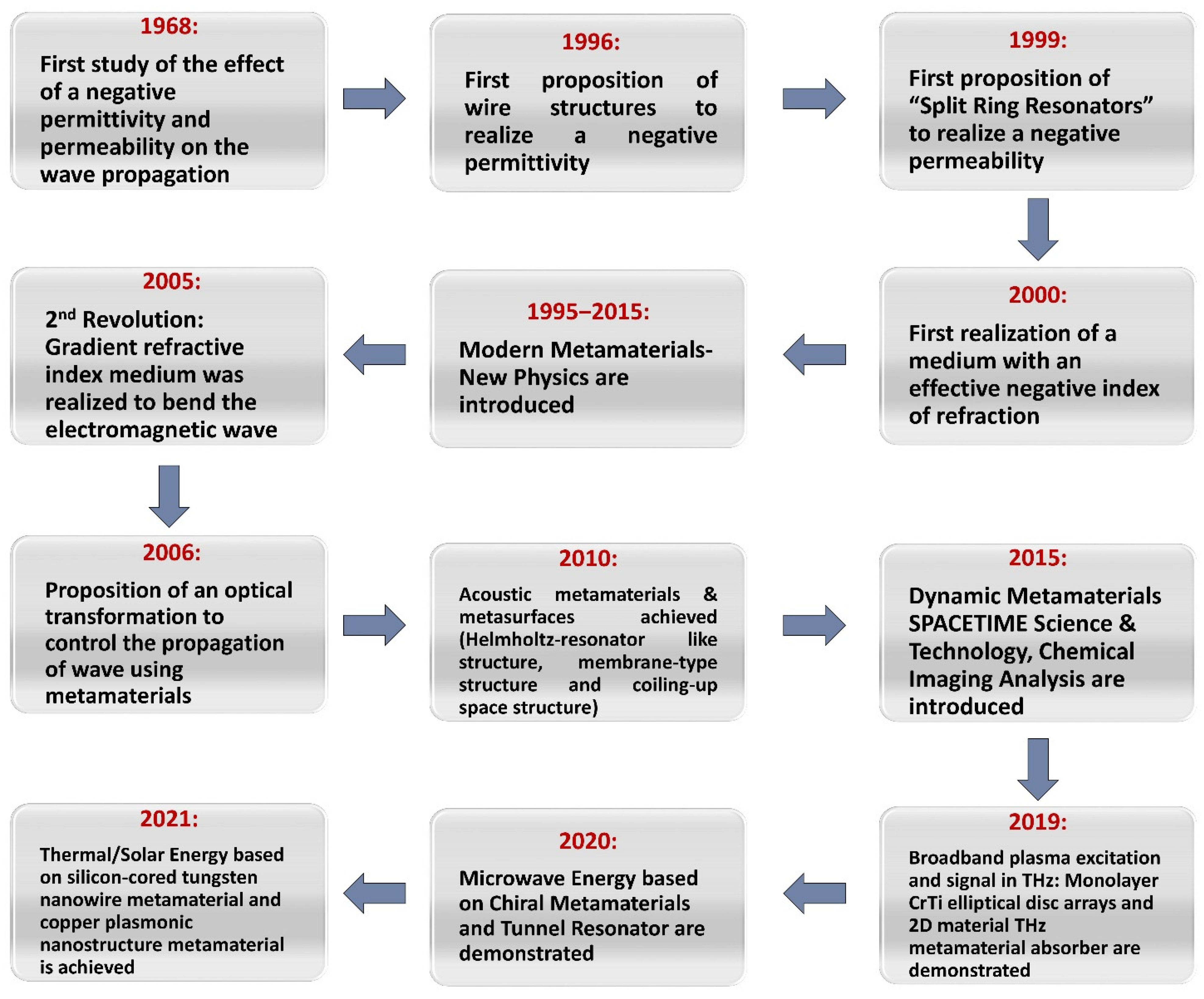
Metamaterials are a type of composite material that combine various elements such as plastics and metals to create artificial structures with unique electromagnetic properties. The term ”metamaterial” comes from the Greek language and refers to something that is superior or beyond. The concept of metamaterials was first proposed by Russian theorist Veselago in 1968. He suggested that it was theoretically possible to create a material with negative permeability and permittivity. This idea was later realized by Pendry et al. in 1999 with the development of the split-ring resonator (SRR) structure. The SRRs are made of metallic rings with gaps, and although they are made of non-magnetic materials, they can respond strongly to magnetic fields.
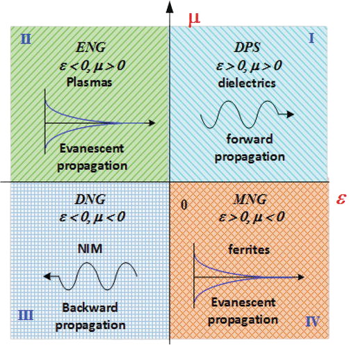
By adjusting the geometric parameters of the SRRs, a band of negative permeability can be achieved in the desired frequency range. Smith et al. took this idea a step further in 2000 by combining two sets of resonators to create both negative permeability and permittivity in the same frequency band. In 2005, Smith demonstrated a new type of left-handed material with both negative permeability and permittivity simultaneously. Metamaterials were initially developed for use in resonant antenna production by Lucent Technology in 2002. Over time, their potential for creating unusual electromagnetic characteristics became apparent, and in 2010 they were used for artificial media structure. Today, metamaterials are used in a wide range of applications, including satellite antenna production, thanks to the development of software that enables the creation of metamaterial- based antennas commercially.
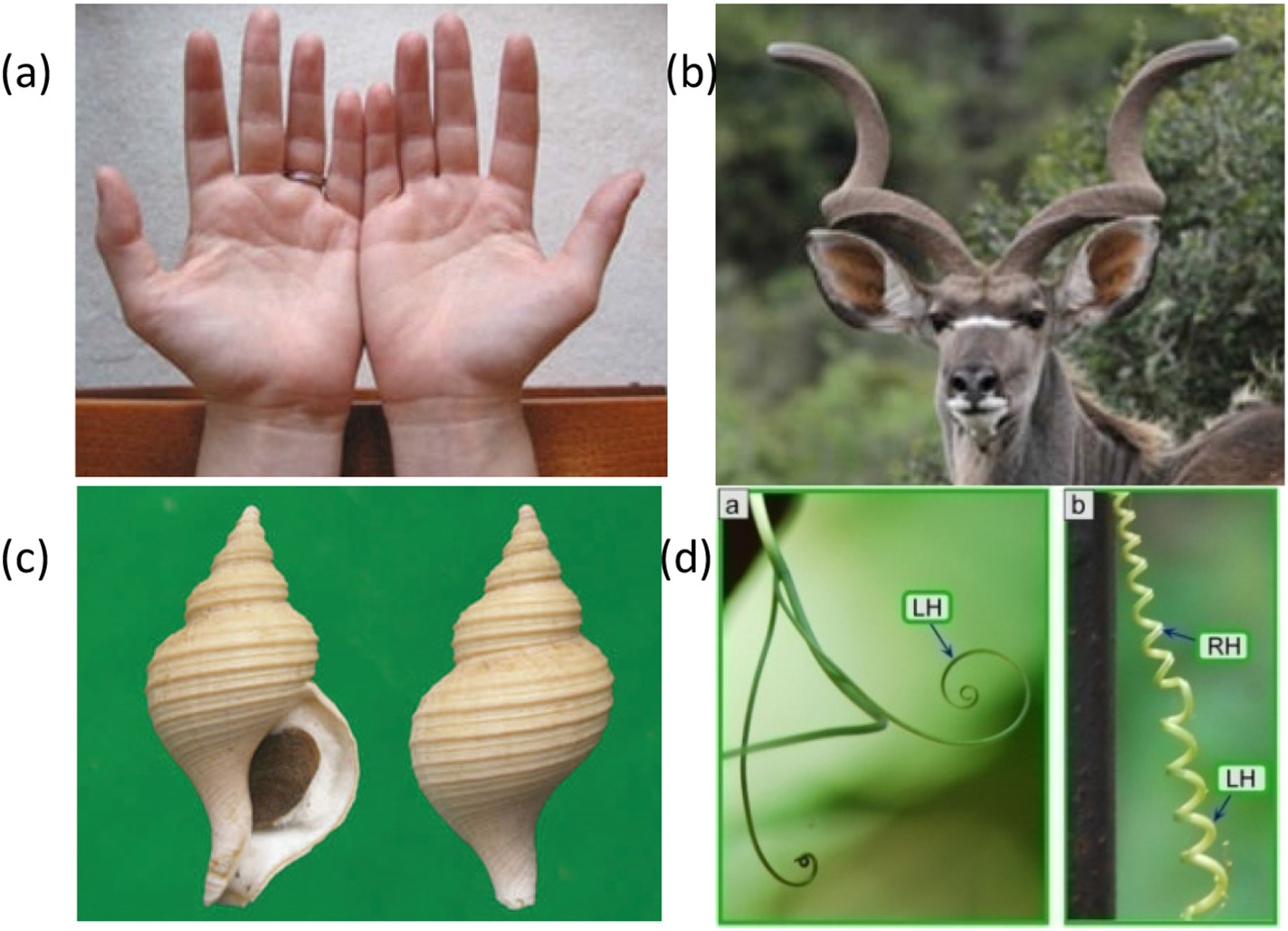
Chirality in metamaterialsA chiral medium is one that displays a unique response to left and right circularly polarized waves due to its intrinsic chiral asymmetry. The concept of chirality was first introduced by Lord Kelvin in 1873, who described it as a geometrical figure that cannot be superimposed onto its mirror image.
It was Pasteur in the 1840s who confirmed the handedness nature of the molecules in optically active materials. In the 1910s, Lindeman succeeded in bringing the optical activity phenomenon in visible light to radio waves by using a collection of helical coils to create artificial chiral ’molecules’. In 2003, Tretyakov and his team suggested the fabrication of a metamaterial composed of chiral particles, such as helical wires, to achieve negative refraction by chiral nihility. The authors proposed that the refractive index for one circular polarization could be made negative through chirality, even if the chiral parameter is small, as long as the permittivity and permeability of the medium are small and very close to zero.
Pendry, in 2004, discussed the possibility of achieving negative refraction in chiral metamaterials. Unlike regular metamaterials, chiral metamaterials do not require both electric and magnetic resonances to have negative epsilon and negative. As long as the chiral parameter is large enough, negative refraction can be obtained in chiral metamaterials, without the need for negative permittivity or permeability. Pendry proposed a practical model of a chiral metamaterial that worked in the microwave regime, with twisted Swiss rolls as elemental structures.
Chiral metamaterials are a type of technologically manufactured material that has features that are not present in naturally occurring substances. These materials possess chirality which gives rise to distinct optical and magnetic responses that are crucial for applications in various fields. Chirality is a fundamental property of molecules and materials that arises from their non-superimposable mirror images. In chiral metamaterials, this property is deliberately engineered by arranging subwavelength metallic or dielectric structures in a precise and controlled manner. The resulting materials exhibit unprecedented control over the propagation and manipulation of light, making them highly desirable for applications in telecommunications, sensing, and energy harvesting. The main advantages of chiral metamaterials is their ability to exhibit strong optical activity and CD, which can be tuned over a wide range of frequencies. This makes them ideal for making novel optical devices, slike polarizers, filters, sensors, that are highly sensitive to the chirality of the surrounding environment. Furthermore, chiral metamaterials can be designed to exhibit negative refraction, which enables them to act as superlenses that can resolve features smaller than the diffraction limit.
Over the last few decades, there has been a significant interest among physicists, material scientists, chemists, and engineers in metamaterials, which are composite materials artificially created and possess unusual properties. Metamaterials have evolved into a vast field that covers various aspects of solid materials, such as optical, electrical, magnetic, thermal, and mechanical properties. This includes both linear and nonlinear properties, as well as static and dynamic behavior. Chiral metamaterials have been advancing quickly over the last few years, with operating frequencies increasing from microwave to optical ranges. The development of chiral metamaterials has been accelerated by advancements in basic theory and fabrication techniques, resulting in numerous useful applications in areas such as polarization manipulation, imaging, and detection. Because most biological substances and tissues are chiral, chiral metamaterials are predicted to find higher uses in biological detection. It is critical to integrate and synthesize information from several fields in order to progress chiral metamaterials. To improve the strength of chirality, the field still requires substantial research into both theory and fabrication technique. The future of chiral metamaterials will be focused on obtaining broad bandwidth and great efficiency. Furthermore, while building reconfigurable chiral metamaterials remains difficult, it is critical to address the growing need for active polarization modification in smart detection and communication systems.
Dated: 24th Jan'2k23Designing structures for chiral metamaterials requires a good understanding of their optical properties and the ability to manipulate electromagnetic waves at the nanoscale level. Here are some general steps that can be followed to design structures for chiral metamaterials:
• Determine the desired chiral response:Chiral metamaterials are characterized by their ability to interact with circularly polarized light in a manner that depends on the handedness of the polarization. The desired chiral response should be determined based on the intended application, such as polarization filtering, chiral sensing, or optical activity.
• Choose a suitable building block:Chiral metamaterials are typically composed of subwavelength building blocks that exhibit strong chiroptical properties. Examples include chiral nanoparticles, helical structures, and planar metamolecules. The choice of building block should be based on the desired chiral response and the fabrication method.
The unit cell is the smallest repeating structure in a metamaterial. It should be designed to exhibit the desired chiroptical properties based on the chosen building block. This may involve optimizing the dimensions and orientation of the building block, as well as the spacing between adjacent building blocks.
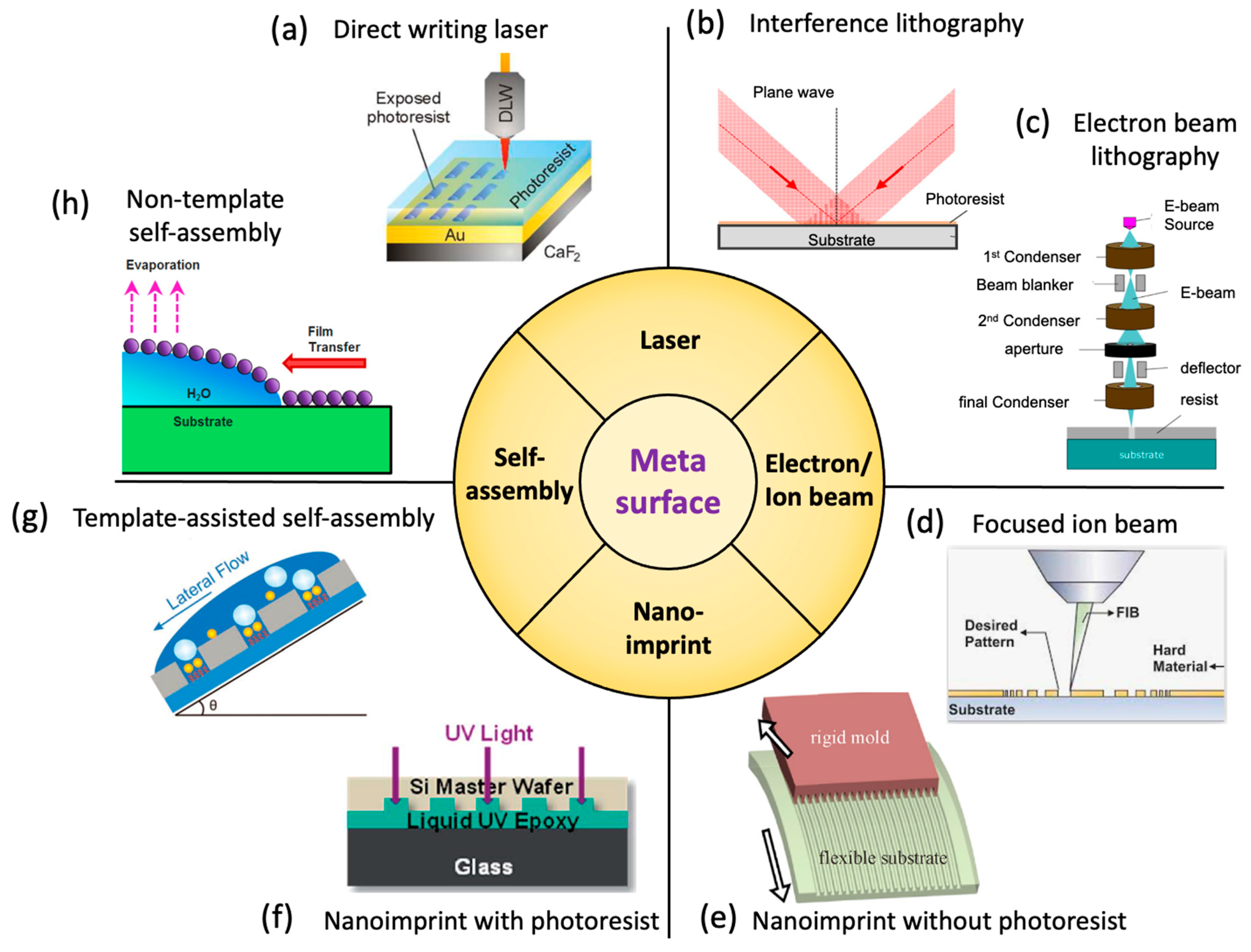
• Fabricate the metamaterial:Chiral metamaterials are typically fabricated using techniques such as electron beam lithography, focused ion beam milling, or nanoimprint lithography. The choice of fabrication method should be based on the desired resolution, throughput, and cost.
• Characterize the metamaterial:The chiroptical properties of the metamaterial should be characterized using techniques such as circular dichroism spectroscopy or polarization-resolved microscopy. This will allow the performance of the metamaterial to be evaluated and any necessary adjustments to be made.
• Optimize the design:The design of the metamaterial can be optimized based on the characterization results. This may involve adjusting the building block dimensions or orientation, changing the unit cell geometry, or using a different building block altogether. Overall, the design of chiral metamaterials requires a combination of theoretical modeling, experimental charac- terization, and optimization to achieve the desired chiroptical properties.
The materials used to make chiral metamaterials can vary depending on the specific design and application. However, some commonly used materials include:
•Metals (such as gold, silver, and aluminum) -These are often used as the building blocks for chiral metamaterials due to their strong optical response and ease of fabrication.
• Dielectric materials (such as silicon and glass) -These materials are used to support and stabilize the metallic chiral structures, and can also be used to create chiral structures on their own.
• Polymers -Polymers can be used to create chiral structures with high flexibility and tunability, making them attractive for applications such as sensing and drug delivery.
• Liquid crystals -Liquid crystals can be used to create chiral structures with tunable optical properties, making them useful for applications such as displays and optical filters. Overall, the choice of materials for chiral metamaterials depends on factors such as the desired optical response, fabrication method, and application requirements.
The fabrication methods for metamaterials are classified into two general approaches: top-down and bottom-up.
The top-down approach involves slicing or systematically and preferentially cutting a bulk material into the final
desired nano-sized shape/geometry; on the other hand, in the bottom-up approach, the buildup takes place from
the bottom atom by atom, molecule by molecule, or cluster by cluster, escalating upward to the final desired
shape. The top-down approach used for the fabrication of nanosized shapes and geometries that is the most
prevalent in the electronic industry is known as lithography. On the other hand, in the bottom-up approach, only
one technique, known as self-assembly, is used.
Electron beam lithography (EBL) is a technique for creating patterns by directing an electron beam onto an electron-sensitive material called a resist polymer. This process involves the use of various lenses, beam distortions, and orifices to control the direction and motion of the electron beam and focus the radiation onto the resist polymer.
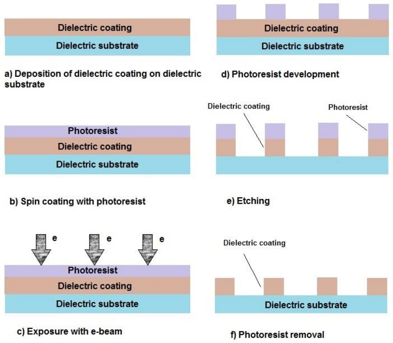
EBL is effective for creating structures smaller than 100 nanometers, making it ideal for producing
metamaterials of similar sizes to visible light wavelengths. The EBL device typically consists of a chamber,column, and objective lenses, as well as electronic components such as a power supply, vacuum pump, computer,
and control units.
•Focused ion beam lithography
The focused ion beam (FIB) method has evolved significantly and become a useful tool for various processes such as lithography, etching, deposition, and doping. The FIB method generally uses liquid metal ion sources such as Ga and Au-Si-Be alloys due to their stability and long lifespan, allowing for the production of electronic devices smaller than a micrometer. The FIB method offers advantages such as high radiation sensitivity to resist polymer, low ion dispersion, low backscattering from the substrate, and better resistance to magnetic fields compared to the EBL method.
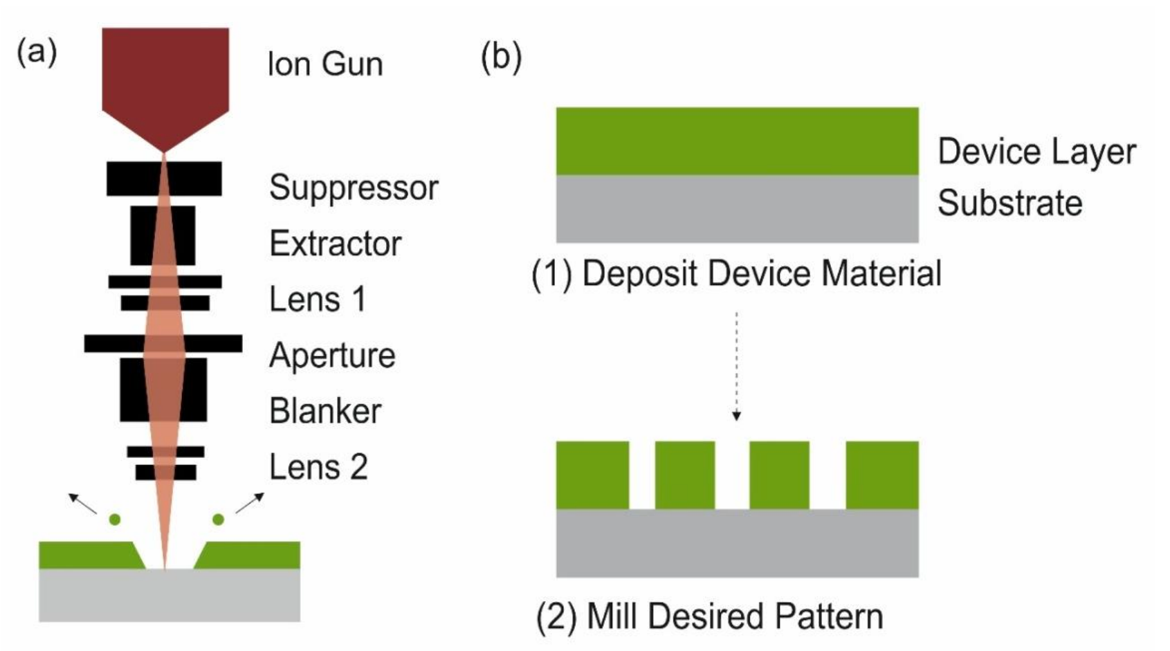
However, the FIB method also has some disadvantages, such as substrate damage and lower
performance. Nonetheless, the FIB method is suitable for cases where substrate damage is not a significant issue.
The FIB method has many benefits for creating and processing magnetic nanostructures, particularly for small
patterns and sheet substrates. The method involves an ion gun with a liquid metal source heated to its melting
point, which is then ionized and accelerated onto the substrate to create desired patterns by FIB milling, leading
to the removal of excess material. Notably, the FIB method does not require a mask.
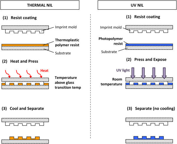
This technique involves pressing a mold with a specific surface pattern onto a substrate covered with a thin layer
of imprint resist polymer, using a pressure of 5-10 MPa. To ensure the polymer fills the mold pores, it’s heated to
a temperature 90-100°C above its glass transition temperature (Tg). Once the pressure is removed and the mold
is taken away, a thin layer of polymer is left on the substrate, which can be removed using reactive ion etching.
There are three types of NIL processes: thermal, UV, and roll-to-roll.
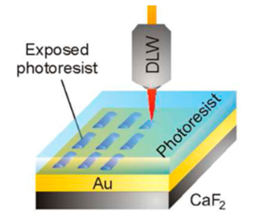
•Laser lithography
The development of large-area fabrication techniques with high precision, flexibility, and uniformity is desir-
able. Two maskless laser-based methods for processing micro- and nanostructures quickly and inexpensively are
laser-direct-write (LDW) lithography and laser-interference lithography (LIL). LDW lithography projects desired
nanopatterns directly onto photoresist using computer-controlled optics, allowing for nano-fabrication of materi-
als that are difficult to mechanically machine and the creation of 3D surface profiles. While LDW lithography
provides a compromise between feature size and processing cost, it is not a batch process. LIL uses interference of
coherent laser beams to produce large-area periodic nanostructures and is a batch process that is limited to peri-
odic patterns. Advanced LIL techniques can create complex periodic nanostructures using multiple exposures and
non-co-planar beams, making it a large-area, high-efficiency, and inexpensive maskless technique that can produce
broadband and high-efficiency reflective linear polarization converters composed of 2D complex nanostructures.
Self assembly
Self-assembly is a process in which an irregular system of components is converted to an organized patterned structure via local interactions among the primary components without applying any external force. Because the driving force for this process ends to reduce its Gibbs free energy and balances the opposing forces of repulsion and attraction, the system reaches a general and local thermodynamic equilibrium after the formation of the structure. To scientifically define the process, it should be stated that self-assembly is a bottom-up method in which atoms or molecules arrange themselves into a regular nanostructure. The formation of salt crystals and snowflakes with complex structures are two common natural examples of self-assembly. In self-assembly, arrangement of nanoparticles or molecules into ordered nanostructures occurs because of their unique electronic, magnetic, catalytic and/or other physical and chemical properties. There are two types of self-assembly processes for nanostructure components: physical and chemical. Physical self assembly is a simple process for creating non-complex structures, and expectedly, there is a lack of long-term stability in thus-assembled nanoparticles. On the other hand, in chemical self-assembly, a strong chemical bonding/coupling usually exists within the nanoparticles and even with the substrate surface, whether functionalized or non-functionalized.A visible-wavelength metamaterial fabricated by self-assembly is schematically shown in figure.
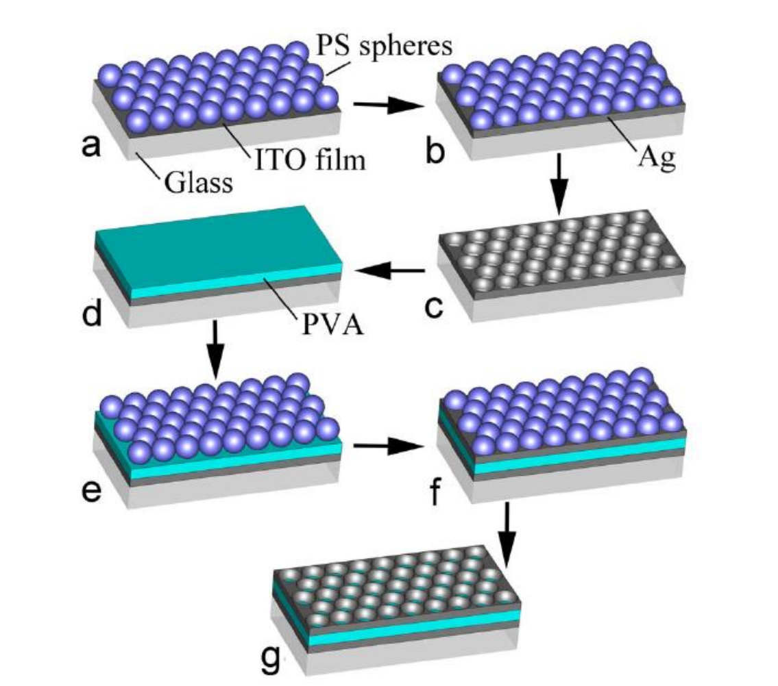
For this fabrication, nano-size polystyrene (PS) spheres were periodically arranged on an indium tin oxide (ITO) glass substrate, followed by deposition of a silver layer into the gaps among the PS spheres.
The PS spheres were removed by washing with chloroform and alcohol, leaving behind a perforated silver film. A polyvinyl alcohol (PVA) solution was spin-coated onto the silver film and solidified in a dry box. Then a second layer of PS spheres was periodically arranged on the solidified PVA film, followed by depositing a second silver layer in the gaps. Again, the PS spheres were removed by washing with chloroform and alcohol, resulting in a three-layered Ag-PVA-Ag sandwich nanostructure.
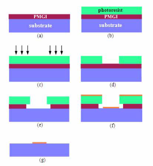
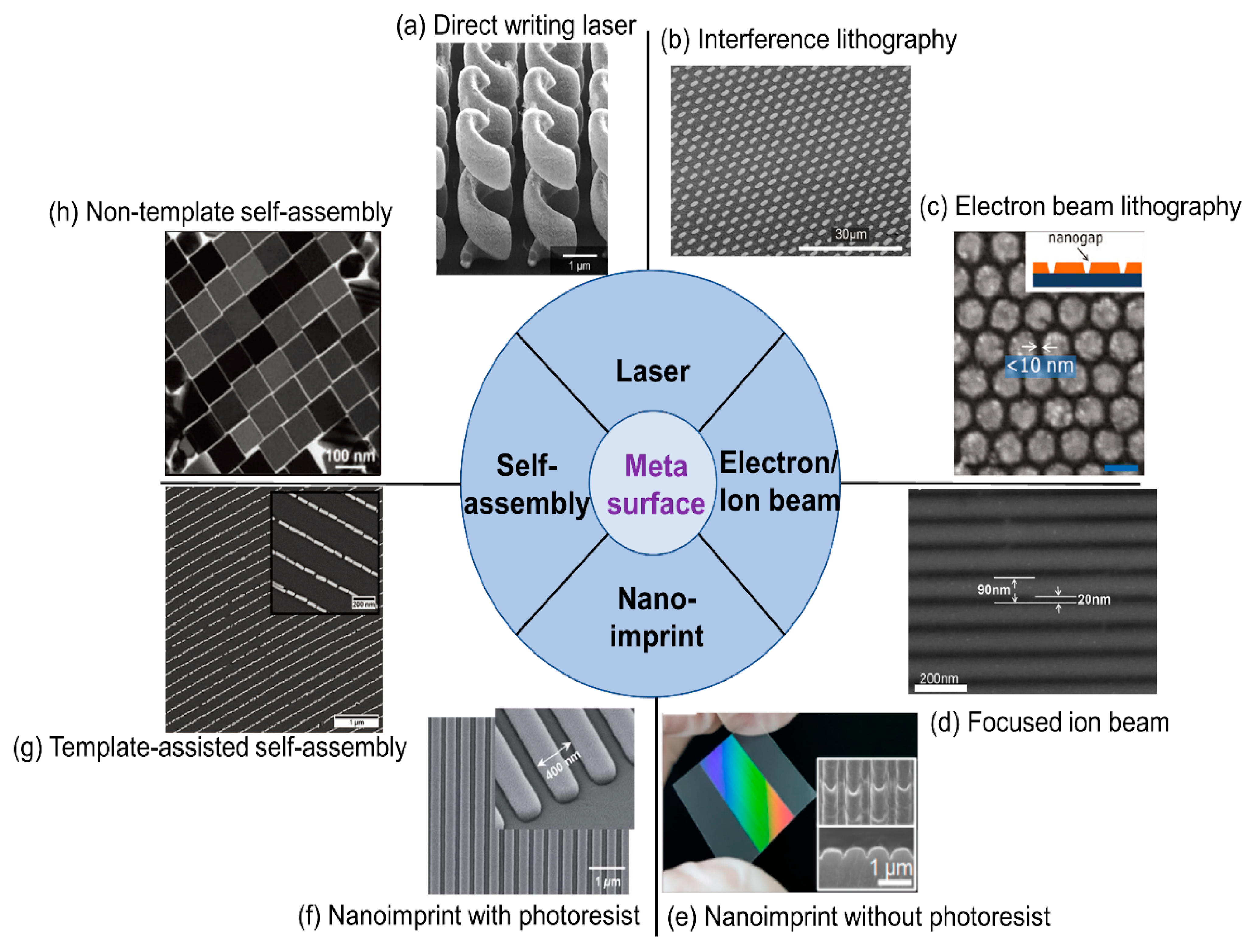
Here we can see all the methods with the gold(AU) materials and their SEM images.
Chiral metamaterials are being developed for a wide range of applications in fields such as optics, electronics, and biomedicine. Here are some examples of applications of chiral metamaterials:
Optical polarizers:
Chiral metamaterials can be used to create optical polarizers that are more efficient than traditional polarizers. These polarizers can be used in displays, cameras, and other optical devices.
Chiral sensors:
Chiral metamaterials can be used to create highly sensitive sensors for detecting chiral molecules. These sensors can be used in medical diagnosis, drug development, and environmental monitoring.
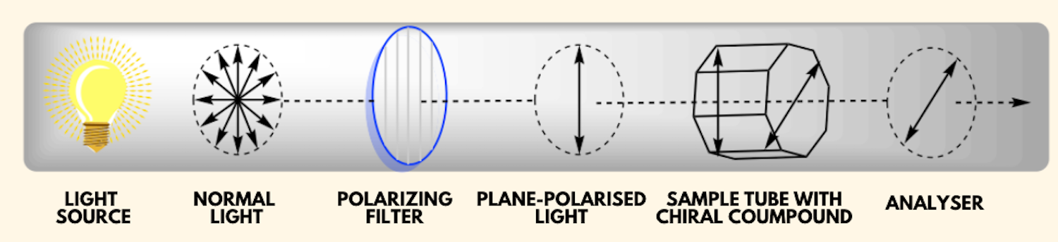
Circular dichroism spectroscopy:
Chiral metamaterials can be used in circular dichroism spectroscopy, a technique used to study the structure of chiral molecules. This technique has applications in the pharmaceutical industry, where it is used to study the interaction between drugs and proteins.
Chiral lenses:
Chiral metamaterials can be used to create lenses that can focus circularly polarized light. These lenses have potential applications in telecommunications, where they can be used to improve the efficiency of data transmission.
Chiral metamaterials for cloaking:
Chiral metamaterials have been proposed as a way to create cloaking devices that can make objects invisible to certain wavelengths of light. This technology has potential applications in military and surveillance industries.
Chiral metamaterials for energy harvesting:
Chiral metamaterials can be used to create energy harvesting devices that can convert waste heat into electrical energy. This technology has potential applications in the automotive industry, where it can be used to improve the fuel efficiency of vehicles.
Overall, chiral metamaterials have a wide range of potential applications in various fields, and ongoing research is expected to lead to further developments in the future.
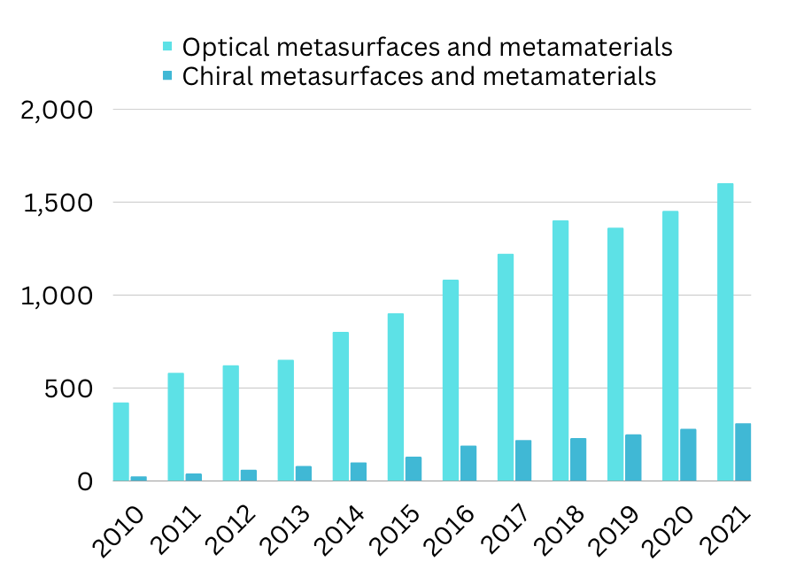
Historial developments in the research artilcles published in the area of optical metasurfaces and chiral metasurfaces is shown in the below diagram. From the figure it was shown that from 2018-19, oprtical metasurfaces articles were approximately equal then afterwards increased but in chiral metasurfaces is consistantly increasing and from 2023 to 2030 , high chances to increase more.
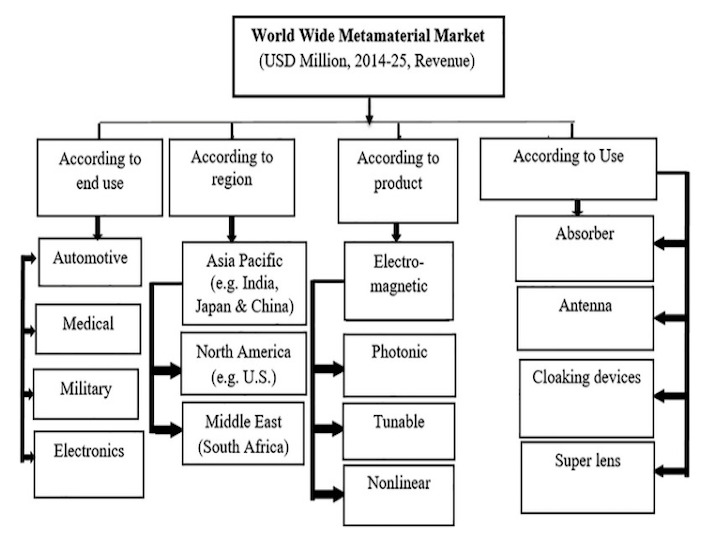
The global market for metamaterials was valued at USD 316 million in 2016, but there is now an increasing demand for high-quality, durable components, which is driving growth in the market. A recent report predicts that the metamaterials market will reach $1.5 billion by 2025, with a compound annual growth rate of 24.8 % between 2020 and 2025. This growth is attributed to the superior properties of metamaterials, which make them attractive to a variety of industries including aerospace, automotive, defense, electronics, public safety, and high-frequency communication applications such as metamaterial antennas in the battlefield.
In the future, there are several potential advancements that could further enhance the capabilities of chiral
metamaterials. These include:
Current chiral metamaterials are typically designed to exhibit a specific optical property, such as circular dichroism or optical activity. In the future, it may be possible to
engineer chiral metamaterials that exhibit multiple optical properties simultaneously, making them more versatile
and useful in a wider range of applications.
Chiral metamaterials could be integrated with other technologies,
such as microfluidics, to create new types of sensors and devices. For example, chiral metamaterials could be used
to create highly sensitive biosensors that can detect small concentrations of biomolecules in a fluid sample.
Currently, the optical properties of chiral metamaterials are fixed once they are fab-
ricated. In the future, it may be possible to develop chiral metamaterials that are more tunable, allowing their
optical properties to be adjusted in real-time in response to changing conditions.
The fabrication of chiral metamaterials is currently a complex and expensive
process that typically requires the use of specialized equipment. In the future, new fabrication techniques may
be developed that make it easier and more cost-effective to produce chiral metamaterials.
Overall, the future of chiral metamaterials is promising, and further advancements in this field could lead to new
and exciting applications in a wide range of industries.
In conclusion, metamaterials are a type of composite material with unique electromagnetic properties that were first proposed in 1968 by Veselago. The development of the split-ring resonator structure in 1999 by Pendry et al. allowed for the creation of materials with negative permeability and permittivity. Metamaterials have since been used in a wide range of applications, including satellite antenna production, due to their unusual electromagnetic characteristics.
Chiral metamaterials, which respond uniquely to left and right circularly polarized waves, were first proposed by Tretyakov and his team in 2003. Unlike regular metamaterials, chiral metamaterials do not require negative permittivity or permeability to achieve negative refraction. Pendry proposed a practical model of a chiral metamaterial that worked in the microwave regime, with twisted Swiss rolls as elemental structures.
Various fabrication methods such as lithography and nanoimprint lithography have been used to create metamaterials, and self-assembly techniques have also been explored with their SEM images.The metamaterial market has grown significantly in recent years, with increasing numbers of articles published each year on the topic.
Future challenges for metamaterials include improving their efficiency, scalability, and durability, as well as reducing their cost and developing new applications. Overall, metamaterials have the potential to revolutionize a wide range of industries and technologies, and continued research and development in this field is likely to yield significant advances in the years to come.
It is with great pleasure that I express my deep appreciation, sincere gratitude, and profound sense of indebted- ness to my seminar supervisor, Professor Shobha Shukla, for his unwavering support and inspirational guidance throughout the course of this research endeavor. Additionally, I extend my gratitude to T. Archana for her invaluable mentoring. This work has presented me with an opportunity to explore a wide range of research areas. Furthermore, I wish to convey my thanks to the department of Metallurgical Engineering and Materials Science (MEMS) at the Indian Institute of Technology Bombay for providing me with such a unique and rewarding seminar experience.
[1] I. Fernandez-Corbaton, C. Rockstuhl, P. Ziemke, P. Gumbsch, A. Albiez, R. Schwaiger, T. Frenzel, M. Kadic,
and M. Wegener (2019). “New twists of 3D chiral metamaterials,” Adv. Mater. 31, 1807742.
[2] Wong, Z. J., Wang, Y., O’Brien, K., Rho, J., Yin, X., Zhang, S., . . . Zhang, X. (2017). Optical and acoustic
metamaterials: superlens, negative refractive index and invisibility cloak. Journal of Optics, 19(8), 084007.
[3] Lindell I V, Sihvola A H, Tretyakov S A and Viitanen A J (1994). Electromagnetic Waves in Chiral and
Bi-isotropic Media (Boston, MA: Artech House Publishers)(Book).
[4] Ma, X., Huang, C., Pan, W., Zhao, B., Cui, J., Luo, X. (2014). A Dual Circularly Polarized Horn Antenna in
Ku-Band Based on Chiral Metamaterial. IEEE Transactions on Antennas and Propagation, 62(4), 2307–2311.
[5] Yogesh, N., Fu, T., Lan, F., Ouyang, Z. (2015). Far-Infrared Circular Polarization and Polarization Filtering
Based on Fermat’s Spiral Chiral Metamaterial. IEEE Photonics Journal, 7(3), 1–12.
[6] Hasan, M. M., Faruque, M. R. I., Islam, M. T. (2018). Dual Band Metamaterial Antenna For
LTE/Bluetooth/WiMAX System. Scientific Reports, 8(1).
[7]Karaaslan, M., Bakir, M. (2014). Chiral metamaterial based multifunctional sensor applications. Progress
In Electromagnetics Research, 149, 55–67.
[8] Lee, Y. Y., Kim, R. M., Im, S. W., Balamurugan, M., Nam, K. T. (2019). Plasmonic metamaterials for
chiral sensing applications. Nanoscale.
[9] Fei Guo, C., Sun, T., Cao, F., Liu, Q., Ren, Z. (2014). Metallic nanostructures for light trapping in energy-
harvesting devices. Light: Science Applications, 3(4), e161–e161.
[10] Lin, K.-T., Lin, H., Yang, T., Jia, B. (2020). Structured graphene metamaterial selective absorbers for high
efficiency and omnidirectional solar thermal energy conversion. Nature Communications, 11(1).
[11] Decker, M., Klein, M. W., Wegener, M., Linden, S. (2007). Circular dichroism of planar chiral magnetic
metamaterials. Optics Letters, 32(7), 856.
[12] Ma, X., Huang, C., Pu, M., Hu, C., Feng, Q., Luo, X. (2012). Multi-band circular polarizer using planar
spiral metamaterial structure. Optics Express, 20(14), 16050.
[13] Plum, E., Fedotov, V. A., Zheludev, N. I. (2008). Optical activity in extrinsically chiral metamaterial.
Applied Physics Letters, 93(19), 191911.
[14] Tretyakov, S., Nefedov, I., Sihvola, A., Maslovski, S., Simovski, C. (2003). Waves and Energy in Chiral
Nihility. Journal of Electromagnetic Waves and Applications, 17(5), 695–706.
[15] Pendry, J. B. (2004). A Chiral Route to Negative Refraction. Science, 306(5700), 1353–1355.
[16] Monzon, C., Forester, D. W. (2005). Negative Refraction and Focusing of Circularly Polarized Waves in
Optically Active Media. Physical Review Letters, 95(12).
[17] Plum, E., Zhou, J., Dong, J., Fedotov, V. A., Koschny, T., Soukoulis, C. M., Zheludev, N. I. (2009).Metamaterial with negative index due to chirality. Physical Review B, 79(3).
[18] Liu, Z., Fang, N., Yen, T.-J., Zhang, X. (2003). Rapid growth of evanescent wave by a silver superlens.Applied Physics Letters, 83(25), 5184–5186.
[19] Fang, N. (2005). Sub-Diffraction-Limited Optical Imaging with a Silver Superlens. Science, 308(5721),
534–537.
[20] Liu, Z., Durant, S., Lee, H., Pikus, Y., Fang, N., Xiong, Y., . . . Zhang, X. (2007). Far-Field Optical Superlens.
Nano Letters, 7(2), 403–408.
[21] Wegener, M. (2013). Metamaterials Beyond Optics. Science, 342(6161), 939–940.
[22] Kern, C., Kadic, M., Wegener, M. (2017). Experimental Evidence for Sign Reversal of the Hall Coefficient
in Three-Dimensional Metamaterials. Physical Review Letters, 118(1).
[23] Wang, B., Zhou, J., Koschny, T., Kafesaki, M., Soukoulis, C. M. (2009). Chiral metamaterials: simulations
and experiments. Journal of Optics A: Pure and Applied Optics, 11(11), 114003.
[24] Huang, X., Lai, Y., Hang, Z. H., Zheng, H., Chan, C. T. (2011). Dirac cones induced by accidental degeneracy
in photonic crystals and zero-refractive-index materials. Nature Materials, 10(8), 582–586.
[25] Ying Cui , Xiaosai Wang, Huan Jiang and Yongyuan Jiang(2022).High-efficiency and tunable circular dichro-
ism in chiral graphene metasurface ,J. Phys. D: Appl. Phys. 55 135102.
[26] Li, J., Yang, F.-Q., Dong, J.-F. (2011). Design and simulation of L-shaped chiral negative refractive index
structure. Progress In Electromagnetics Research, 116, 395–408.
[27] Ye, W., Yuan, X., Guo, C., Zhang, J., Yang, B., Zhang, S. (2017). Large Chiroptical Effects in Planar Chiral
Metamaterials. Physical Review Applied, 7(5).
[28] Mart ́ın Rodr ́ıguez, Ernesto Mu ̃noz, Juan Garcia-Collado, Angel Margineda, J. Barba, Ismael Gomez
Gomez, Alvaro Molina-Cuberos, Gregorio. (2013). Design and Characterization of Chiral Metamaterials
using Numerical Simulations Tools.
[29] Ijaz, S., Rana, A. S., Ahmad, Z., Zubair, M., Massoud, Y., Mehmood, M. Q. (2022). The Dawn of Metade-
vices: From Contemporary Designs to Exotic Applications. Advanced Devices Instrumentation, 2022, 1–24.
[30] Ali, A., Mitra, A., A ̈ıssa, B. (2022). Metamaterials and Metasurfaces: A Review from the Perspectives of
Materials, Mechanisms and Advanced Metadevices. Nanomaterials, 12(6), 1027.
[31] Bhattacharya, S., Saha, C., Siddiquiand, J.Y. (2019). High Frequency Applications of Metamaterials and
Metasurfaces. 2019 IEEE Recent Advances in Geoscience and Remote Sensing : Technologies, Standards and
Applications (TENGARSS), 96-99.
. . . . . . . . . . . . . . . . . . . . . . . . . . . . . . . . . . . . . . . . . . . . . . . . . . . . . . . . . . . . . . . . . . . . . . . . . . . . . . . . . . . . . . . . . . . . . . . . . . . . . . . . .
• CD : Circular Dichroism
• OA : Optical Activity
• MST : Multiple Scattering Theory
• LCP : Left Circularly Polarised Light
• RCP : Right Circularly Polarised Light
• PCMM: Planar Chiral Metamaterials
• CDT : Circular Dichroism in Transmission
• LSPR: Localised Surface Plasmon Resonance